Euraudio LDA17 (LDA17mk3, LDA17mk2, LDA172, LDA162) specifications
Welcome to the Euraudio LDA17 specifications, in which you can read about the system requirements (application criteria), operation and technical data of the LDA17. The information applies to the LDA17mk3, LDA17mk2, LDA172 and LDA162, too.
The LDA17 is an ultra low distortion, low noise, mono, transistor audio amplifier, intended for use with high performance home audio loudspeakers, but it can be used as a reference or measurement amplifier as well. LDA17mc is the medium power version of the amplifier, capable of max. 80 Watts per 4 ohms output power. LDA17hc is the high power version of the amplifier, capable of max. 120 Watts per 4 ohms output power. LDA17xc is the extra high power version of the amplifier, capable of max. 200 Watts per 4 ohms output power. Please find the LDA17mc, LDA17hc, and LDA17xc assembly instructions here.
LDA17 system requirements
LDA17 is just a power amplifier circuit, it doesn't contain power supply and protection circuits, however there are Euraudio DiY kits that do. LDA17mc is part of the stereo Euraudio LDA MIN DiY kit. LDA17hc is part of the stereo Euraudio LDA MID and dual mono Euraudio LDA DM1 DiY kits. LDA17xc is part of the dual mono Euraudio LDA DM2 DiY kit and is part of the mono Euraudio LDA MON DiY kit.
The amplifier wasn't tested with switch-mode power supplies. LDA17mc, LDA17hc, and LDA17xc can be used with your own conventional power supply, the only requirement is that the supply should be dual (symmetric) and its unloaded voltage should be between +/-30...36 V for the LDA17mc, it should be between +/-30...42 V for the LDA17hc, and it should be between +/-30...52 V for the LDA17xc (for 4 ohms load).
Higher supply voltage is not recommended, and it wasn't tested, but let's mention it. If you can ensure that the load impedance is never lower than the minimum load impedance shown in the technical data below, then you may raise the unloaded supply voltage of the LDA17mc up to +/-48 V, the unloaded supply voltage of the LDA17hc up to +/-54 V, and the unloaded supply voltage of the LDA17xc up to +/-60 V.
In the case of LDA17xc, you may even apply up to +/-68V supply voltage, if you install a bigger heatsink for the driver transistors, and change the supplied 63 V electrolytic capacitors that are in the rail and rail filter lines to ones with higher withstanding voltage (e.g. 80 V or 100 V). These capacitors are:
LDA17: C7, C11, C13, C15; LDA172: C7, C10, C15, C17; LDA162: C9, C11, C15, C18.
Operation
The LDA17 has a 3-stage transistor amplifier structure. It consists of the input, voltage amplifier (VAS) and output stages. It mostly follows the concept that was set forth in the books of Douglas Self and Robert Cordell, and what Douglas Self called a blameless amplifier. For now, I decided not to publish the exact circuit of the LDA17 on this home page, but here's a simplified blameless amplifier schematic from page 98 of Douglas Self's book, "Audio Power Amplifier Design Handbook", 5th edition.
A short overview of the simplified circuit

The input stage is a differential amplifier (TR2, TR3) fed by the current source (TR1) and loaded by the current mirror (TR10, TR11) as well as the input (TR12) of the voltage amplifier TR4. Degeneration resistors R2, R3 make the input stage much more linear. In the VAS, TR12 is often called a beta enhancer. It's purpose is to provide high impedance at the VAS input. The current mirror and TR12 together make the input stage see a very high impedance at its output, and consequently the input stage gain will be high. The voltage amplifier also has a current source (TR5), and consequently has quite high gain, which is only degraded somewhat by the input impedance of the output stage. The high gains of the input and VA stages provide an open loop gain of about 120 dB (1,000,000) at low frequencies. Dividing by the closed loop gain of about 30 dB (LDA17hc), there is still plenty of signal available for the negative feedback to correct the nonlinear output stage. The double emitter follower ("EF2") output stage is biased in the low distortion region between class B and class AB. The driver transistors (TR6, TR8) always work in class A, due to the shared emitter resistor R15. The overall negative feedback is stabilized by dominant pole frequency compensation (C3 Miller capacitor).
TPC versus Miller compensation
In the actual LDA17 (LDA172, LDA162) circuit, the J4 (TPC) jumper serves to select two-pole frequency compensation instead of the traditional Miller compensation. With TPC compensation, lower distortion was measured at high frequencies.
Maximum ratings
Allowed max. sinusoidal output power: 200 Watts (LDA17xc); 120 Watts (LDA17hc), 80 Watts (LDA17mc) see derating curve for testing purpose.
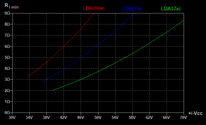
Allowed minimum load impedance versus unloaded supply voltage (with adequate heatsinking):
Technical data
At 25°C ambient temperature unless otherwise noted.
Input sensitivity: -10 dBV (316 mV RMS)
Input impedance @ 1kHz: 15.8 kohms (LDA17xc); 13.5 kohms (LDA17mc and LDA17hc)
Input impedance @20 kHz: 7 kohms ± 15%
Voltage amplification: 29.5 dB (LDA17xc), 28 dB (LDA17mc and LDA17hc)
Frequency response (-3dB):
5 Hz to 280 kHz (with 100 ohm source impedance)
Signal to noise ratio (without hum): > 114 dB @ 200 W/ 4 ohms (LDA17xc); > 113 dB @ 120 W/ 4 ohms (LDA17hc); > 112 dB @ 80 W/ 4 ohms (LDA17mc)
Slew rate: > 15 V/us
Damping factor (1kHz, 8 ohms): > 200
Typical distortion data*
Total harmonic distortion @1 kHz: THD < 0.001% (2 Watts into 4 ohms)*
Total harmonic distortion @10 kHz (48 kHz bandwidth): THD < 0.004% (2 Watts into 4 ohms)*
Intermodulation distortion (19 kHz:20 kHz = 1:1): IMD < 0.005% (2 Watts into 4 ohms)*
Transient (dynamic) intermodulation distortion (Square wave 3.15 kHz + sine wave 15 kHz): DIM < 0.005% (2 Watts into 4 ohms)*
* With TPC jumper installed. Distortion depends on many factors that are in the hands of the DiY builder, such as cable routing, PCB positioning, construction and vicinity of the power transformer, etc. 2 Watts into 4 ohms were chosen because the crossover distortion tends to be the most significant in this output voltage range. Distortion is similarly low at all other power levels.