Euraudio CTA12 and CTA14(A) specifications
Welcome to the Euraudio CTA12 and CTA14(A) specifications, in which you can read about the system requirements (application criteria), operation and technical data of the CTA12 and CTA14(A).
The CTA12 and CTA14(A) are low distortion, mono, transistor audio amplifiers, intended for use with high performance home audio loudspeakers. CTA12 is capable of max. 50 Watts output power, while CTA14(A) is capable of max. 100 Watts output power. Please find the CTA12 and CTA14(A) assembly instructions here.
CTA12 and CTA14(A) system requirements
The CTA12 and CTA14(A) are just power amplifier circuits, they don't contain power supply and protection circuits, however there are such Euraudio DiY kits, like the Euraudio PS1US and PS1S power supply kits and the Euraudio SMRS/SMRSx switch-on thump mute kit that can be used with the CTA12 and CTA14(A).
The amplifier wasn't tested with switch-mode power supplies. CTA12 and CTA14(A) can be used with your own conventional power supply, if it is dual (symmetric) and its unloaded voltage is at least +/-26 V for the CTA12 and at least +/-30 V for the CTA14(A) and not more than the "Absolute limits of unloaded supply voltage" given in the Maximum ratings section below. The maximum unloaded supply voltage may be further limited by the "Minimum permissible load impedance" specified in the Maximum ratings.
Recommended unloaded supply voltage: +/-29V (CTA12), +/-37V (CTA14, CTA14A), this ensures that the amplifier is not overloaded even with a 4 ohm speaker impedance.
Operation
The CTA12 and CTA14(A) has a 3-stage transistor amplifier structure. It consists of the input, voltage amplifier (VAS) and output stages. It mostly follows the concept that was set forth in the books of Douglas Self and Robert Cordell, and what Douglas Self called a blameless amplifier. For now, I decided not to publish the exact circuit of the CTA12 and CTA14(A) on this home page, but here's a simplified blameless amplifier schematic from page 98 of Douglas Self's book, "Audio Power Amplifier Design Handbook", 5th edition.
A short overview of the simplified circuit

The input stage is a differential amplifier (TR2, TR3) fed by the current source (TR1) and loaded by the current mirror (TR10, TR11) as well as the input (TR12) of the voltage amplifier TR4. Degeneration resistors R2, R3 make the input stage more linear. In the VAS, TR12 is often called a beta enhancer. It's purpose is to provide high impedance at the VAS input. The current mirror and TR12 together make the input stage see a very high impedance at its output, and consequently the input stage gain will be high. The voltage amplifier also has a current source (TR5), and consequently has quite high gain, which is only degraded by the input impedance of the output stage. The high gains of the input and VA stages provide an open loop gain of about 106 dB (200,000) at low frequencies. Dividing by the closed loop gain of 26 dB, there is still plenty of signal available for the negative feedback to correct the nonlinear output stage. The output stage in the CTA12 and CTA14(A) actually consist of power darlington transistors biased in the low distortion region between class B and class AB. The overall negative feedback is stabilized by dominant pole frequency compensation (C3 Miller capacitor).
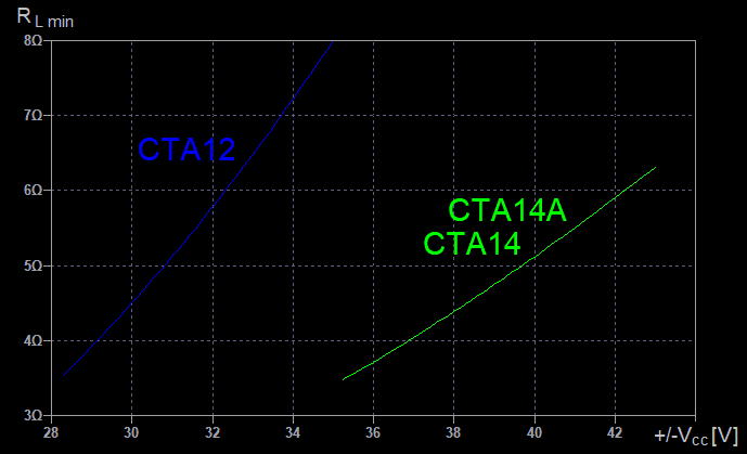
Maximum ratings
Absolute limits of unloaded supply voltage: +/-35V (CTA12); +/-42V (CTA14, CTA14A)
Allowed max. sinusoidal output power: 50 Watts (CTA12); 100 Watts (CTA14, CTA14A) see derating curve for testing purpose.
Minimum permissible load impedance versus unloaded supply voltage (with adequate heatsinking):
Technical data
At 25°C ambient temperature unless otherwise noted.
PCB size: 90x48 mm (CTA12), 90x58 mm (CTA14), 90x59 mm (CTA14A)
Input impedance @ 1 kHz: 24 kohms ±10% (CTA12), 29 kohms ±10% (CTA14, CTA14A)
Input impedance @20 kHz: 11 kohms ±25%
Voltage amplification: 26 dB (CTA12), 28.5 dB (CTA14, CTA14A)
Frequency response (-3dB):
8 Hz to 150 kHz (with 100 ohm source impedance)
Damping factor (1kHz, 8
ohms): > 150
Typical distortion data, CTA12*
Total harmonic distortion @1 kHz: THD < 0.0015% (2 Watts into 6 ohms)*
Intermodulation distortion (250 Hz : 8 kHz = 4:1): IMD < 0.012% (2 Watts into 6 ohms)*
Transient (dynamic) intermodulation distortion (Square wave 3.15 kHz + sine wave 15 kHz): DIM < 0.01% (2 Watts into 6 ohms)*
Typical distortion data, CTA14(A)*
Total harmonic distortion @1 kHz: THD < 0.0015% (2 Watts into 4 ohms)*
Intermodulation distortion (250 Hz : 8 kHz = 4:1): IMD < 0.01% (2 Watts into 4 ohms)*
Transient (dynamic) intermodulation distortion (Square wave 3.15 kHz + sine wave 15 kHz): DIM < 0.01% (2 Watts into 4 ohms)*
* Distortion depends on many factors that are in the hands of the DiY builder, such as cable routing, PCB positioning, construction and vicinity of the power transformer, etc. 2 Watts into 4 ohms or 6 ohms were chosen because the crossover distortion tends to be the most significant in this output voltage range. Distortion is similarly low at other power levels.